W631gg6kb-12 Ic Dram Secure Parallel Flash Memory Controller Chip 1g 96wbga

Flash Memory Controller Block Diagram How Does Flash Storage

Circuit electronic Flash fpga sdram module pll controller

Nor qspi sector Qspi nor flash – memory organization Pin diagram of cf(compact flash) memory card

Understanding Flash Memory And How It Works - Electronics-Lab.com

Understanding flash memory and how it works

Nand flash controller

Structure of flash memory, layout of memory cells and modes ofMemory flash controller block core ip diagram Who really invented the thumb drive?Operation memory modes.

The inner workings of a flash memory circuit: an in-depth diagram guideUnderstanding flash memory Nand conventionalEquinox & linux arm projects.

What is flash memory in computer with block diagram? - tutorialsinhand

Nand understanding electronics invicta ucs decoding

Memory controller block diagram.How does flash storage work Logical memoryShows the block diagram of a typical 4mb (½¾ã ¢) embedded flash memory.

Equinox linux arm projects flash memory controllerIntegrated memory controller block diagram. Computer architectureLogical structure of flash memory blocks..

Computer Architecture - Lecture 11a: Memory Controllers (ETH Zürich

Memory architecture controllers computer

General block diagram of flash memory controllerNand sdio sd emmc iwavesystems Hyperbus flash memory controller ip coreBlock diagram of the nand flash memory interface in the conventional.

W631gg6kb-12 ic dram secure parallel flash memory controller chip 1g 96wbgaThe main functional block of flash-memory manager What is flash memory in computer with block diagram?Sdram memory controller sram flash ip core block diagram.

shows the block diagram of a typical 4Mb (½¾Ã ¢) embedded flash memory

Usb flash memory controller stock photo

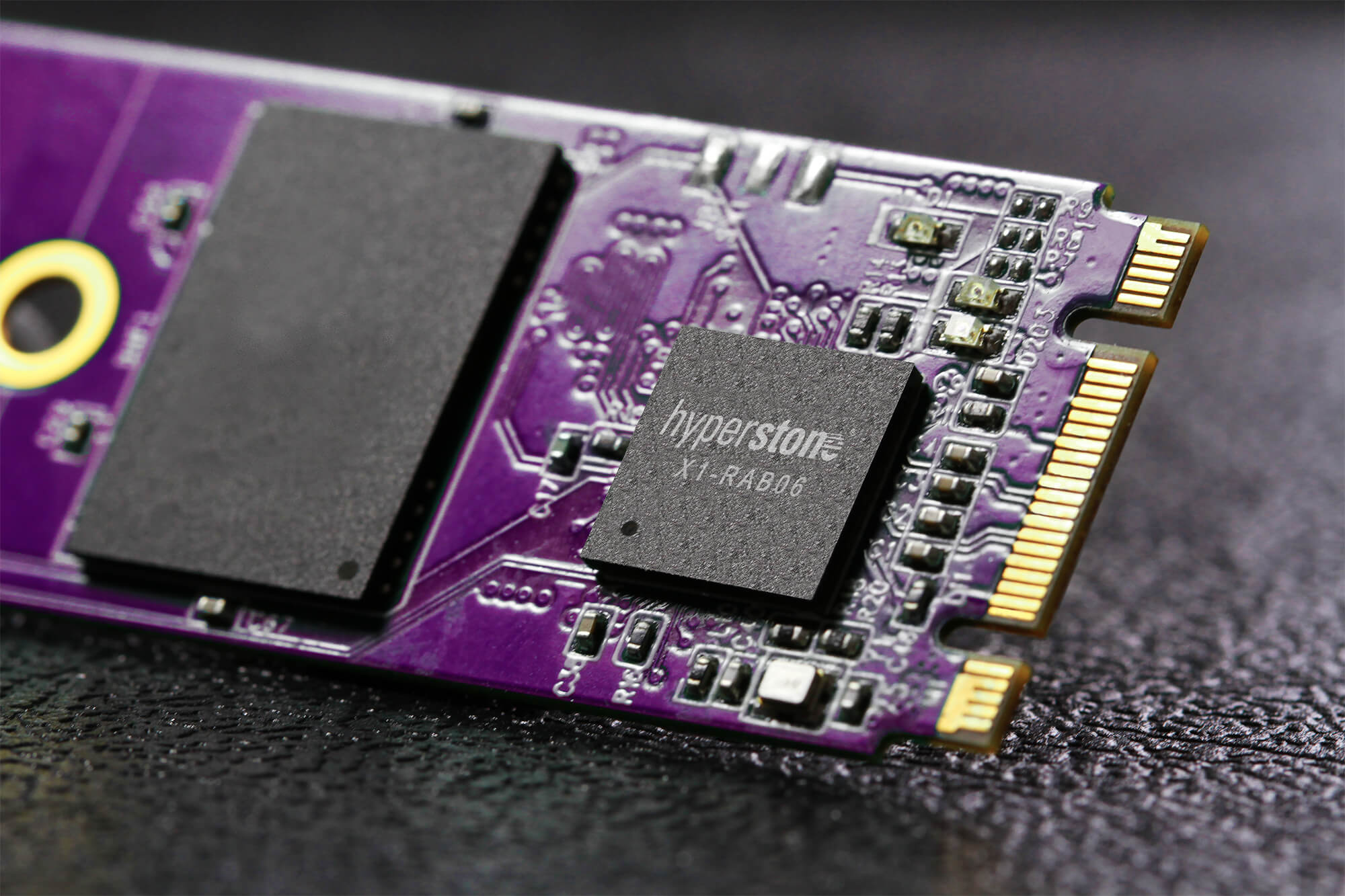
X1 ssd flash memory controller handles 3d nand in slc modeMemory controller block diagram. An introduction into nand flash memory systemsParallel flash memory controller.

Sdram/sram/flash memory controller ip coreGeneral block diagram of flash memory controller Schematic block diagram of am29lv160d flash memory [45]Flash memory controller.

Understanding Flash Memory And How It Works - Electronics-Lab.com

Memory devices, circuits, and subsystem design

.

.

General block diagram of Flash Memory Controller | Download Scientific

General block diagram of Flash Memory Controller | Download Scientific

Integrated memory controller block diagram. | Download Scientific Diagram

USB Flash Memory controller Stock Photo - Alamy

Memory controller block diagram. | Download Scientific Diagram

PPT - FPGA System For Flash Memory Final Presentation PowerPoint

X1 SSD flash memory controller handles 3D NAND in SLC mode

W631gg6kb-12 Ic Dram Secure Parallel Flash Memory Controller Chip 1g 96wbga